Closer look at image intensifiers
I.I. is an image intensifying tube primarily developed for night vision under starlight. A typical I.I. has a vacuum envelope made of ceramic in which a photocathode for converting light into electrons, a microchannel plate (MCP) for multiplying electrons, and a phosphor screen for reconverting electrons into light are arranged in close proximity. Optically connecting an I.I. to an industrial camera allows imaging low-light-level phenomena including not only visible light but also invisible light in the near infrared and UV regions. A gate function can also be added as an electronic shutter to perform high-speed imaging.
Structure and operation of I.I.
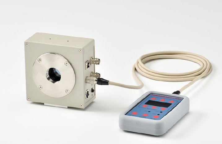
The C14245 series is a family of cubic, compact, lightweight I.I. units designed to easily connect to most types of cameras.
Operating an I.I. requires a high-voltage power supply circuit providing about 8000 volts and a control circuit. To make I.I. easier to handle and use, Hamamatsu Photonics has produced I.I. units assembled in conjunction with the necessary peripheral circuits. Those I.I. units have been used mainly with a compact CCD camera for low-light-level imaging in industry, biology, astronomy, and academic research fields, etc. Meanwhile, cameras have been greatly improved with higher performance and more diverse shapes and sizes. This increases the need for I.I. units that connect to various types of cameras even more easily than the conventional I.I. units that usually have a relatively large L shape configuration.
By rethinking the circuit layout and overall structural design to arrange the necessary circuits together around an I.I., Hamamatsu Photonics successfully fabricated a cube-shaped unit that easily connects to the body of various cameras and power cables. At the same time, the company redesigned the electronic components and changed the circuit design to reduce the cubic volume and overall weight down to two-thirds that of conventional I.I. units. The cube-shaped design has a good weight balance that helps relieve mechanical stress on the connected camera. The C14245 series I.I. units in this way eliminate restrictions on the shape and size of camera to connect to and so will extend applications of low-light-level imaging and observation even to the invisible range, such as for imaging faint electrical discharges from poor insulation points on printed circuit boards, combustion status in engines, and cell fluorescence.
Hamamatsu Photonics will currently release three models of C14245 series I.I. units having sensitivity in different spectral ranges from UV to near infrared. Hamamatsu Photonics also provide higher sensitivity models that use a two-stage MCP for electron multiplication and will continue developing still more compact units that allow observing even more fast-changing phenomena.
Features of this product
1. Easily connectable to various types of cameras
The company redesigned the circuit layout and structure of the entire unit to relocate the required components around the I.I. periphery. This enabled to fabricate a cube-shaped unit that easily connects to the body of most cameras and power cables. The cube-shaped design has a good weight balance that relieves the mechanical stress on the connected camera or microscope.
2. Compact and lightweight
Besides taking a close look at previously used electronic components and then employing smaller components, Hamamatsu Photonics devised the peripheral circuit design with dimensions slashed to 100mm×100mm×45mm (W×H×D) and a weight of only about 600 grams, so the cubic volume and weight are reduced to about two-thirds that of conventional I.I. units.


