The Quantum Revolution
Quantum technology will change the world. Based on groundbreaking research results, numerous players from science and industry are already working on a variety of completely new applications. Politicians have also recognized the disruptive potential of quantum technology and its social dimension and have launched major funding programs. Hence, revolutionary technological developments can soon be expected in the fields of quantum optics, quantum communication, quantum sensor technology and, in particular, quantum computing.
But the quantum revolution will only take place as long as there is a practical platform technology for quantum devices and quantum systems. The quantum computers that exist today consist of complex opto-electronic designs and are very sensitive to the smallest external influences. The quantum registers used there only operate at temperatures close to absolute zero and require highly intricate cooling. Another challenge is the connection to the existing information and communication technology. In the long term, such large-scale solutions are of greater interest for research purposes or for commercial cloud computing providers. In contrast, industry and small and medium-sized enterprises would have a high demand for their own supercomputers for a variety of complex simulation tasks and optimization problems that could be perfectly solved by quantum computing.
Solid-State Devices as a Gamechanger?
A way out of this dilemma is offered by quantum devices whose quantum bits consist of so-called color centers. Quantum bits, or qubits for short, represent the smallest quantum information unit. A color center is a special atomic defect in the crystal structure in which a single lattice atom is missing. Alternatively, a color center can be a cluster of a few impurities in the material where impurity atoms replace lattice atoms. Since the impurity can absorb and emit light, it is called a color center. Quantum information can then be stored in the electron spin of these color centers.
Currently, the wide-bandgap (WBG) semiconductor material diamond is particularly prominent and well researched. Diamond has excellent quantum properties, but this material is technologically difficult to handle and the integration with established electronic technologies is demanding. There are also efforts to realize qubits using classical silicon technology, sometimes in combination with germanium or graphene. The advantage: The complete range of proven semiconductor processes would be available for silicon-based quantum devices, and integration into established silicon electronics would be comparatively simple. That said, silicon is not a WBG semiconductor and therefore has less optimal characteristics as a base material for quantum devices.
Under these circumstances, solid-state devices based on the WBG semiconductor material silicon carbide (SiC) could open the way for quantum technology in broad fields of application. SiC-based semiconductor devices are now mass-produced. Currently, SiC components are proving their qualities in practical use, especially in the field of power electronics.
As in diamond, in SiC the quantum information can be stored in the spins of the color centers. But unlike diamond, SiC combines the highly attractive quantum properties with a mature material platform. The SiC platform offers, for example, commercial availability on a wafer scale, very good compatibility with established CMOS technology (CMOS: Complementary Metal Oxide Semiconductor) or the possibility to produce hybrid photonic, electron and mechanical devices.
Isotope Controlled Silicon Carbide
Color centers in SiC can be used for quantum information processing, quantum sensing or quantum communication. Such applications, however, require relatively long lifetimes of the quantum states, for example for the realization of complex computational tasks. In SiC, this can be achieved by transferring quantum information from a color center to the nuclear spins of neighboring silicon (Si) or carbon (C) atoms.
Not every Si or C atom in SiC is suitable as a quantum bit or memory. Only certain isotopes such as Si-29 and C-13, which occur in varying concentrations in SiC, can be used for this purpose. In current quantum research, isotopic concentrations that occur naturally in SiC have been investigated, or SiC material that does not contain such storage isotopes.
In contrast, Fraunhofer IISB focuses specifically on optimized material quality tailored to the respective quantum application. With its many years of expertise in the field of SiC epitaxy and a highly developed process technology, the institute approaches the production of epitaxial SiC layers with precisely defined isotope concentrations on SiC substrates. In this respect, the IISB is one of the few institutions worldwide that will be able to produce SiC material with properties specified exactly for the respective quantum application.
It's the Dose that Counts
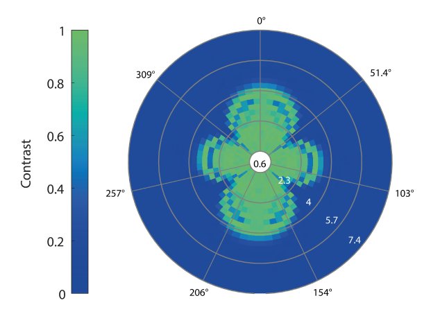
A key criterion in the use of SiC as a quantum material is the optimal amount and placement of the special isotope atoms in relation to the central color center. Too low an isotope concentration will result in a lack of coherence of the qubits, while too high a concentration will cause overlapping signals, which would make it difficult to differentiate the states of the qubits. The distribution of isotope atoms is directly related to the isotope concentrations in SiC. By means of sophisticated computer simulations, the IISB investigates which isotope concentration in SiC is best suited for applications in quantum communication or quantum computing. Using a numerical algorithm developed in-house, the signal quality of the nuclear spins can be determined as a function of their position relative to the respective central color center.
The best isotope positions can be found in a shamrock-shaped area around the color center. In this case, the “shamrock” must be populated by an optimal number of nuclear spins, which can be achieved by setting a specific isotope concentration. The key to producing SiC optimized for quantum applications therefore lies in the precise control of the isotope concentrations.
Things are Better Together!
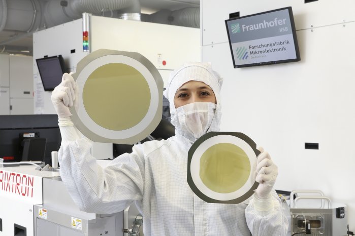
In the manufacturing of the optimized SiC, Fraunhofer IISB can rely on many years of expertise in the field of epitaxy on both Si and SiC substrates. For example, the institute in Erlangen operates the world's first planetary epitaxy reactor for 150 and 200 mm SiC wafers at a research facility. For several years, Fraunhofer IISB has maintained a strategic cooperation with the company AIXTRON in the development of SiC equipment and processes. AIXTRON is a leading global supplier of equipment for SiC epitaxy using the chemical vapor deposition (CVD) process. The two partners maintain a Joint Lab in a clean room at the IISB to develop epitaxy equipment and processes together. The “Joint Labs“ model allows intensive synergies to be realized between industry and science. For the institute, the cooperation with AIXTRON represents an ideal opportunity to expand its activities in the field of industrial SiC epitaxy development like few other research institutions. AIXTRON, in turn, benefits from the direct integration into the IISB clean room technology line and the extensive characterization and analysis capabilities on site. In addition, both partners can share the high technological and personnel effort that is due to the extreme quality requirements for the material. By working directly with a renowned industrial company in house, the IISB can produce very special epitaxial layers for high-end demonstrator devices, which commercial suppliers cannot offer in this way.
Fraunhofer IISB explicitly wants to produce not only for its own needs, but also to give other organizations access to high-quality SiC substrates and to provide the research community with optimal base materials for quantum applications. SiC substrates with alternative crystal orientation, such as so-called "a-plane" material, are already being developed for this purpose.
From Material to System
The IISB's extensive epitaxy activities are embedded in the institute's strategy of offering research services along the entire value chain – from semiconductor materials to power electronic systems. The technological foundation for this is a continuous and industry-compatible CMOS process line for Si wafers up to 200 mm and SiC wafers up to 150 mm in diameter. As part of the joint initiative "Forschungsfabrik Mikroelektronik Deutschland" (FMD, Research Fab Microelectronics Germany), this CMOS line is currently being qualified for 200 mm SiC wafers. Within FMD, Fraunhofer IISB has established itself as a competence center for SiC and is consistently expanding its activities in this field. With the process line, the IISB also benefits from advanced technologies for heterointegration and patterning on the nanometer scale. The work of the IISB's Hybrid Integration department on packaging and interconnection technology, for example for extreme environmental conditions such as cryogenic environments, complements the technological portfolio.
Due to its holistic approach, the IISB can apply its know-how and process technology from the field of power electronic SiC devices to solid-state quantum electronics. Accordingly, the focus is not only on the optimized base material, but also on the development of technological processes for the manufacturing of defined point defects or color centers in SiC. Beyond quantum computing the technological processes are also designed to enable quantum sensing and communication devices and applications. In this context, the long-standing cooperation with the Chair of Electron Devices (LEB) at FAU Erlangen-Nürnberg is particularly worth mentioning. The LEB chair holder Prof. Jörg Schulze is also the director of the IISB; and with Prof. Roland Nagy, an authority on the theory and design of quantum devices in the solid state was recently recruited for the chair. In recognition of his research project on the realization of a SiC-based quantum computer network, Prof. Nagy recently received a grant from the Federal Ministry of Education and Research (BMBF). The funding measure serves to establish an independent junior research group with which Prof. Nagy realizes new research approaches on SiC quantum devices at the LEB and the IISB.
A Universal Technology Platform for Quantum Electronics
The declared goal of Fraunhofer IISB is to establish SiC as an essential platform for quantum communication, quantum computing and quantum sensing. The advantages are manifold. Since the operating temperature for SiC quantum electronics is at least a factor of 1,000 higher than for current large-scale solutions, in the field of quantum computing compact desktop setups with miniaturized cooling devices are becoming within reach. SiC solid-state quantum devices are compatible with the manufacturing processes of classical Si-based microelectronics, and the entire range of electronic peripherals would be available for SiC-integrated quantum devices. A direct coupling to existing technologies would allow quantum electronics to be seamlessly integrated into existing information systems.
SiC as a material platform offers a realistic prospect for marketable quantum devices and for their integration into established microelectronics technologies. By combining quantum properties with electronic devices, isotope-controlled SiC opens up enormous value-adding potential for quantum electronics.
Fraunhofer IISB's news releases are available online at: https://www.iisb.fraunhofer.de/en/press_media/press_releases.html
There you can also find the image material for editorial use.
This press release is also available in German:
https://www.iisb.fraunhofer.de/de/press_media/pressemitteilungen.html


