The Schmid Group can offer today an innovation package which will only be counted as standard in solar cell production in the coming years and promises efficiency increases of 0.4 to 0.6%abs while at the same time reducing the conversion costs by 6 Euro-Cent/Wp.
Schmid's concept of High Efficiency Metallization Technology (HiMeT) designed for the metallization of the front and rear sides of solar cells achieves ultimate cell efficiency at a minimum of mechanical strain, maximum printing pattern flexibility and a drastically reduced raw material consumption.
This technology permits the processing of ultra-thin wafers at competitive prices.
The future-oriented systems designed for the contact-free metallization of the rear side and the application of a seed layer for the contacts on the front side as well as light-induced electro-plating, can be easily integrated in existing production lines.
Not only the flexibility and the contact-free printing technology, but also the potential saving of silver against the background of increasing raw material prices are the central advantages of the HiMeT concept. With standard electrode layouts the saved amount currently lies at ca. 60 mg. By 2012, in combination with new electrode concepts, the potential saving is expected to reach 80%.
Laser Transfer Printer
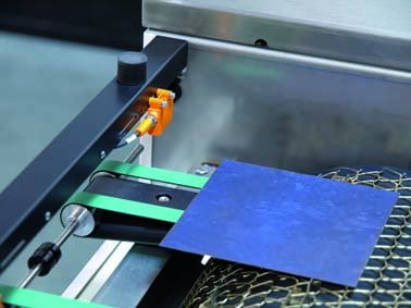
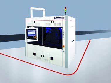
The Laser Transfer Printer (LTP) which won the Intersolar Award 2010, replaces the conventional screen printer in rear-side metallization. Two process features reduce the unwanted stress of sensitive wafers and permit interruption-free production: the contact-free printing eliminates breakages and micro-cracks and the wet-in-wet rear-side metallization reduces the thermal strain thanks to the elimination of a drying step, which in turn brings about the advantage of lower investment costs (CAPEX).
The process is equally precise as it is gentle: a position detector over the vacuum transport band determines the position of each wafer. A fully digitalized print workflow aligns the printing pattern for each wafer. Furthermore, the serialization of printing patterns or changing them at will is also possible.
The laser separates the metal paste drop by drop from the ink ribbon and applies fine structures of 80 µm on mono or multi-crystalline material - and this is achieved at a throughput of up to 1650 wafers per hour. In standard processes a layer of silver for the busbar is applied to the rear side and then a layer of aluminum for the back surface field. But also the application of special patterns for the metal-wrap-through technique or the printing of changing motives for research purposes is no problem for the LTP, thanks to the digital printing technology it features.
Nano Jet
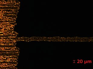
The Nano Jet applies a seed layer as the basis for the subsequent electro-plating of the front-side contacts using inkjet-technology. Innovative printing heads make finger-widths of 35-40 µm possible and that at an excellent contact resistance of less than 3 m?·cm²; the printing pattern can be aligned precisely to the position of the selective emitter as required, using optical position sensors and digital printing technology.
Drying and firing
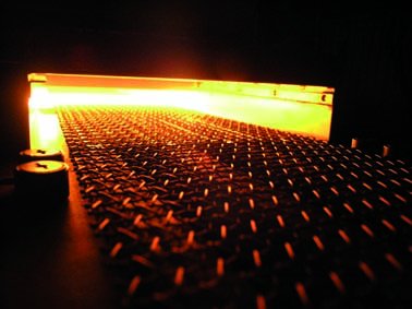
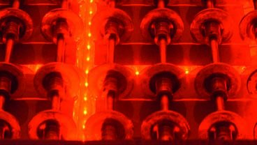
The furnace for drying the rear-side coating and the combined drying and firing furnace for the seed layer originate from the Schmid Group member SierraTherm and are efficient, maintenance-friendly systems offering advantages for both screen printing lines as well as Schmids HiMeT line.
Light-induced plating
In this proven and stable light-induced plating process, silver or an alternative material is applied to the seed layer contact-free to produce the required electrical conductivity of the front-side contacts.
