RISC-V is an instruction set architecture (ISA) based on the reduced instruction set computer (RISC) design principle. Unlike other architectures, RISC-V is a free and open ISA thanks to the Berkeley Software Distribution (BSD) licensing and it is designed for a wide range of application domains. Semiconductor manufacturers can implement their RISC-V-based system on a chip (SoC) in three word-widths, 32, 64, and 128 bits. Furthermore, for the instruction set various subsets can be implemented, which for example offer special functions for embedded systems or integer arithmetic.
In addition to the general instruction set support of the RISC-V architecture for 32- and 64-bit applications, the UDE offers users a whole range of other practical advantages. For example, the available compilers and assemblers for RISC-V use two calling conventions for register names: the standard calling convention, where the register name is prefixed by either “x” or “f”, and the processor specific Application Binary Interface (psABI) with symbolic names. When debugging applications with the UDE, both calling conventions are available to developers in the core register window.
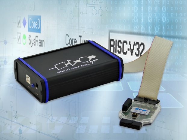
The high-performance microcontroller E31 from SiFive is the first real silicon supported by UDE. This device implements the RV32IMAC instruction set (32-bit, Integer Multiplication and Division Support, Atomic Mode and Compressed Mode). For a fast and reliable debug communication via JTAG to the E31 users can choose between the three devices UAD2pro, UAD2next and UAD3+ of PLS’s Universal Access Device (UAD) family. Since the E31 follows the Arm specification with 10-pins for the physical and electrical implementation of the debug interface, the universal Arm adapter from PLS is used for the connection between the devices of the UAD family and the E31. Galvanic isolation of the debug interface from the UAD is also optionally available. Other devices implementing the RISC-V architecture and which are also supported by UDE are the GD32VF103 series from GigaDevice and the GAP8 ultra-low-power multi-core system-on-a-chip (SoC) from Seeed.
Moreover, with the three variants Cyclone V SE, SX and ST from Intel, the UDE supports a further FPGA-based device family. As so-called system on a chip (SoC) FPGAs, all of these devices offer an integrated hard processor system (HPS) in the form of a single- or dual-core Arm Cortex-A9 processor. This combines the flexibility of an FPGA’s programmable logic with the performance and ecosystem of Arm application processors. The Cyclone V FPGAs minimize power consumption and with an abundance of intellectual property (IP) blocks available customers can tailor the SoC to a wide range of applications in industrial, wireless, broadcast and consumer electronics.
UDE supports application debugging with comprehensive visualization options, among other things. The extensive support for the dual-core variants is particularly user-friendly in practice. For example, both cores are controlled in a single debug session and within a single common debugger instance. In addition to that, developers benefit also from other highly efficient multi-core debug functions, such as multi-core run control for synchronous stopping and starting and multi-core breakpoints that can be used in shared code.


