Visit us at SEMICON West 2012, from July 10th to 12th, in San Francisco, Moscone Center, South Hall, booth # 1641.
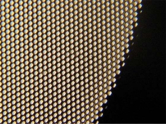
Homogenizers, such as microlens arrays or diffractive optical elements (DOEs), are used in optical systems of semiconductor and flat panel display manufacturing and inspection equipment (e.g. wafer, mask and panel inspection systems, lithography systems for high precision fabrication of small structures). Homogenizers play a prominent role in illumination systems and serve the well defined distribution of light over a particular area in a certain plane of the optical beam path. The optical and micro-optical components used for this purpose also have to meet requirements for a long life time and optimum transmission for short wavelength high energy laser radiation. Compared to other optical materials, CaF2 features a higher damage threshold and thus a better long-time stability of optical performance.
At SEMICON West, Jenoptik is demonstrating it's highly flexible manufacturing capabilities for micro-optical structures in CaF2, especially for wavelength's in the range of 193-266 nm, presenting various CaF2 homogenizer arrangements. With an advanced micro-structuring process in combination with grayscale technology and a sophisticated wafer level etching process, Jenoptik can fabricate customized refractive, diffractive and hybrid structures even with asymmetric shapes and radii. The advantage of this fabrication process is the generation of free geometries, as well as the accuracy and reproducibility of the microstructuring process. This enables a variety of beam distribution patterns and thus opens up new technical solutions where system performance of semiconductor manufacturing equipment needs to be optimized.
In addition, standard manufacturing processes are available for a range of different optical materials such as SiO2, GaAs, GaP, Al2O3, ZnS, ZnSe, Ge, Chalcogenide, etc. Qualified testing at operating wavelength guarantees the quality of optical product properties.
By investing in a modern fabrication environment and specially trained professionals, Jenoptik is recognized as an important development and fabrication partner, offering support throughout the entire development and production process - from design work and prototype manufacturing to the point of serial production.
Practical experience of many years of successful customer projects with international market leaders makes it the ideal partner for challenging, high-quality products for markets such as semiconductor equipment industry, laser material processing, health care & life science or image processing.
About Jenoptik Optical Systems division
Through its Optical Systems division, the Jenoptik Group delivers world class precision optics and systems designed and manufactured to the highest quality standards.
Besides offering customized systems, modules and assemblies, the Optical Systems division is a development and production partner for optical, micro-optical and coated optical components - made of optical glasses, IR materials as well as polymers.
It possesses outstanding expertise in the development and manufacture of optics and microoptics for beam shaping used in the semiconductor industry and laser material processing.
The product portfolio also includes optical and opto-electronic systems and components for applications in defense & security, health care & life science, digital imaging, machine vision as well as lighting.


