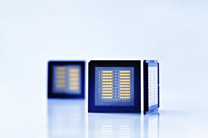
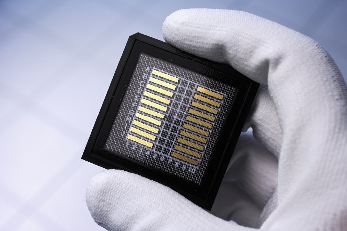
Jenoptik will commission new metallization plants for wafer processing by the beginning of 2020 at the latest. These machines enable various metal layers to be applied to semiconductors by vapor deposition or sputtering. In addition, the so-called lift-off process will be modernized with a new machine. This serves to remove the photoresist mask after exposure on the semiconductors. For the final process step, the facet coating, Jenoptik will also be using a new plant and, simultaneously, a new technology starting in the fall of 2019. This will contribute more strongly to the stabilization and higher output power of laser bars.
The technical modernization of all systems allows for the production of laser diodes with a higher output power and improves reliability. “With the new investments, we want to expand the total production capacity, increase the value added in the process chain and accelerate the worldwide order processing of lasers”, says site manager Dr. Jürgen Sebastian.
Jenoptik’s semiconductor laser bars are mainly used in the fields of medical technology and life science, for example for hair removal, as well as for advanced manufacturing technologies. The investments also serve to address new markets, such as LiDAR sensors in the automotive industry. In the same way, global research and development projects in Europe, Asia and the USA can also be supported thanks to the new production equipment.
Jenoptik facility in Berlin
Jenoptik’s laser production plant was established in 2002 when JENOPTIK Diode Lab GmbH was founded as a spin-off from the Ferdinand Braun Institute, Leibniz Institute for High Frequency Technology (FBH) in Berlin. In March of this year, all activities and businesses were transferred from JENOPTIK Diode Lab GmbH to JENOPTIK Optical Systems GmbH as part of the standardization of corporate structures and processes.
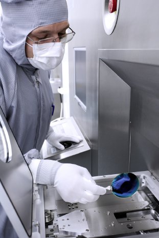
The complete process line for the production of semiconductor lasers takes place in clean rooms with class 100 and 1,000 (ISO 5 and 6) which meet the strict cleanliness requirements for the production of semiconductor lasers and wafers. The wafers are structured and processed into laser bars, which are then delivered to customers worldwide, processed into high-power diode lasers in Jena and integrated into laser systems.
In recent years, the production facility has developed into a state-of-the-art high-tech production facility as a result of various investments. Following an extensive expansion of the process line for the production of semiconductor lasers in 2012, an investment in a new stepper followed last year.


