As a manufacturer of on-chip debuggers (OCDs) and analyzers iSYSTEM has profound know-how on debug interfaces, e.g. NEXUS, ETM, etc. These interfaces are usually called trace ports. Increasing requirements on microcontrollers for higher integration and faster clock rates at less power consumption pose huge challenges on semiconductor as well as tool vendors to guarantee high bandwidths on trace ports. The more a microcontroller is integrated and clocked, the easier the (on-chip trace) signals are distorted. Already at the design a customer can look ahead and enhance the quality of measurement results by deployment of design guidelines.
On-chip debug functionality on most of today's controllers is realized by compressing the CPU activity on-chip and delivering over a trace port to an external tool (e.g. OCD). The tool records the data, analyzes them and displays this information. Physically a trace port consists of data lines and clock line which is used to capture the data in a moment, when it is valid and stable.
The data can be captured on rising edge of the clock ("Full Rate") or on both clock edges ("Half Rate"). At lower frequencies and good signal integrity we can consider the clock and data lines as pure digital signals, which are correctly phase aligned. The OCD can capture the data accurately in this scenario.
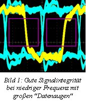
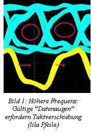
Beside figures show the data and clock signals measured with an oscilloscope.
The data signal is shown in blue, the clock signal is yellow. The different blue lines show one signal at different time periods - the oscilloscope ran in "persistence" mode, so the curves drawn on the oscilloscope's screen are accumulated.
The dark area within the signal is called the data eye - sampling within this region yields a reliable trace recording (Figure 1: pink squares).
However when the frequency rises, the capturing of data becomes challenging due to increased signal integrity issues (noise, skew, crosstalk, reflections, ground bounce...). As shown in Figure 2 with higher frequencies the data eye shrinks (pink circle) and the clock signal has to get shifted (pink arrows).
PCB design flaws like long or different long trace lines, stubs on trace lines, CPU sockets, etc. can distort trace signals up to a point where no correct sampling is possible.
Recommendations
To avoid signal distortion and to retrieve a high quality trace already the PCB designer should consider several aspects.
- The CPU should be soldered on the PCB. Any socket can reduce signal integrity dramatically.
- All trace port lines on the PCB should be as short as possible (max ~2,5 cm),
- Trace lines should run on the same layer or on layers with the same impedance.
- Preferred layer impedance is 50 Ohm.
- Mictor ground pins should be connected directly to PCB's GND plane.
- Trace clock should be serially terminated by 47 Ohm resistor as close as possible to the driver. The value of the resistor may be changed depending on driver characteristics.
- Trace clock should be clean of crosstalk - if possible with double distance to closest nets.
- Trace clock should have only point-to-point connection - any stubs should be avoided.
- It is strongly recommended also for other (data) lines to be point-to-point only. If any stubs are needed, they should be as short as possible. If longer are required, there should be a possibility to optionally disconnect them (e.g. by jumpers).
- Trace port data bus inner crosstalk is not so important, but it is critical to isolate the whole bus from other signals (including from the trace port clock).
More Information
1) Trace Port PCB Design Guidelines In this document you find more examples and details on high frequency effects.
2) How does Autocalibration work?
3) Background information on the "Possibilities and Limits of Software Debugging Techniques Depending on the Microcontroller/Microprocessor"
4) http://en.wikipedia.org/...


