QR code for the current URL

Story Box-ID: 962000

Fraunhofer-Institut für Elektronische Nanosysteme ENAS Technologie-Campus 3 09126 Chemnitz, Germany http://www.enas.fraunhofer.de/
Contact Ms Silvia Hertel +49 371 45001277

Thick Aluminum Layers for Assembly and Packaging Technology

At the SENSOR+TEST 2019, Fraunhofer ENAS introduces an electroplating process to manufacture thick aluminum layers on up to 150 mm substrates

(PresseBox) (Chemnitz, )
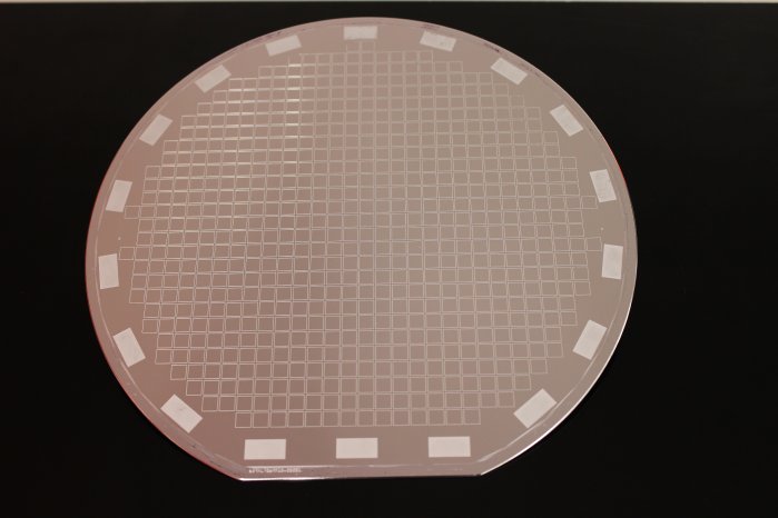
Within a public funded project (AioLi BMBF-FKZ: 16ES0329K), the Fraunhofer ENAS developed a deposition process of thick aluminum layers on various substrates, like silicon, printed circuit board or ceramics. Due to the negative standard potential of aluminum, the electrodeposition is carried out in an ionic liquid instead of water-based electrolytes. With this method, it is possible to deposit aluminum layers up to 30 µm on 6-inch substrates. The wafer-level coating is therefore unique in the world.

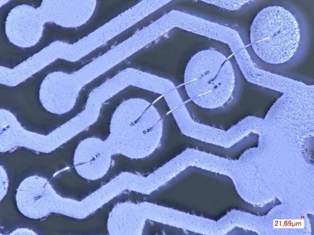
The patterning is done using pattern plating through a resist mask. After the deposition, the seed layer is etched and the patterns are electrically isolated. The layers can be used as conductor paths, heat management, bond pads or bond frames for chip and wafer-level bonding. The electrical properties of galvanically deposited aluminum correspond to those of bulk material to 87 percent. Thus, the properties of the electroplated aluminum are 10 percent better than those of aluminum layers deposited from the gas phase.

Further research and development work is focused on the long-term goal of using galvanic aluminum in both printed circuit board technology and semiconductor technology. Due to its material properties, aluminum is a good alternative to copper in printed circuit boards. In microsystems technology and microelectronics, aluminum is established as final metallization. A homogeneous material system would therefore be feasible with the help of ultrasonic flip chip assembly using aluminum pillars (instead of tin bumps).

The next steps will therefore address assembly and interconnection technology on aluminum surfaces and the coating of topographies, such as through-holes or blind holes, in the printed circuit board and on semiconductor substrates. The scaling of the process to 8-inch wafers or larger rectangular substrates is also being considered. To achieve this, a lot of engineering work has to be done in terms of plant technology in order to scale from laboratory equipment to industrial plants.

For the further development steps, the Fraunhofer ENAS is looking for interested companies, which are interested in a cooperation in the field of electroplated aluminium or just identified an application scenario for the electroplated aluminum. Furthermore, the deposition can be adapted as a service on customer-specific substrates with regard to size, material, seed layers, etc.

At the Fraunhofer joint booth in hall 5 (No. 248), Fraunhofer ENAS will present the process and possible applications of electroplated aluminum.
Website Promotion

Website Promotion

Fraunhofer-Institut für Elektronische Nanosysteme ENAS

The Fraunhofer-Gesellschaft is the leading organization for applied research in Europe. Its research activities are conducted by 72 institutes and research units at locations throughout Germany. The Fraunhofer-Gesellschaft employs a staff of more than 26,600, who work with an annual research budget totaling 2.6 billion euros. Of this sum, 2.2 billion euros is generated through contract research. Around 70 percent of the Fraunhofer-Gesellschaft's contract research revenue is derived from contracts with industry and from publicly financed research projects. International collaborations with excellent research partners and innovative companies around the world ensure direct access to regions of the greatest importance to present and future scientific progress and economic development.

The publisher indicated in each case (see company info by clicking on image/title or company info in the right-hand column) is solely responsible for the stories above, the event or job offer shown and for the image and audio material displayed. As a rule, the publisher is also the author of the texts and the attached image, audio and information material. The use of information published here is generally free of charge for personal information and editorial processing. Please clarify any copyright issues with the stated publisher before further use. In case of publication, please send a specimen copy to service@pressebox.de.
Important note:

Systematic data storage as well as the use of even parts of this database are only permitted with the written consent of unn | UNITED NEWS NETWORK GmbH.

unn | UNITED NEWS NETWORK GmbH 2002–2024, All rights reserved

The publisher indicated in each case (see company info by clicking on image/title or company info in the right-hand column) is solely responsible for the stories above, the event or job offer shown and for the image and audio material displayed. As a rule, the publisher is also the author of the texts and the attached image, audio and information material. The use of information published here is generally free of charge for personal information and editorial processing. Please clarify any copyright issues with the stated publisher before further use. In case of publication, please send a specimen copy to service@pressebox.de.