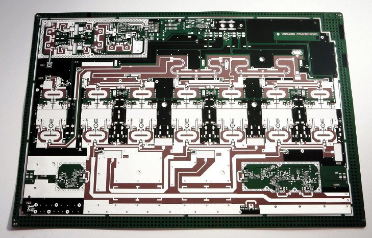
Rohde & Schwarz is one of the biggest and technologically leading European manufacturers of test & measurement equipment. However, the highly specialised services of the Teisnach factory are also available for external customers. Thus, they can make use of the company’s long-term expertise in manufacturing complex PCBs for demanding applications.
The specialists at Rohde & Schwarz Teisnach offer their customers an all-in service: They cross-check the PCB data supplied by the customer and optimise them according to the processes established at the factory. The production flow is automated as far as possible in order to warrant for stable manufacturing quality. Well-engineered registration methods allow for very high packing densities. The following 100% test checks the inner layers against the Gerber data by means of an automated optical inspection (AOI), while the top layers are tested electrically against the network map.
A test coupon per sheet allows for measuring the impedances of RF boards. If the manufacturing involves mechanical processes (like e.g. depth-controlled drilling or milling) or galvanic processes (like e.g. partial gold coating or chemical coating with tin, nickel/gold or silver), then Rohde & Schwarz Teisnach provides and analyses corresponding metallographic cross sections. Further tests, like temperature-change tests, climate tests or soldering tests on reflow soldering lines complete the services.
One of the areas of expertise at Rohde & Schwarz Teisnach are RF multilayer PCBs using a combination of substrates like FR4, PTFE or ceramics. Therefore, the company perceives itself as the undisputed market leader in complex PCBs for RF applications.
More information can be found on the internet: http://www.teisnach.rohde-schwarz.com
<<Background information for editors >>
HDI is the abbreviation of High Density Interconnect and stands for a technology, enabling much narrower conductive tracks and vias than conventional multilayer boards. Because of the HDI microvias, signals can be contacted and disentangled in the inner layers without consuming any valuable space on the top layers. The narrow tracks allow for impedance-controlled conductors for high and highest frequencies.

