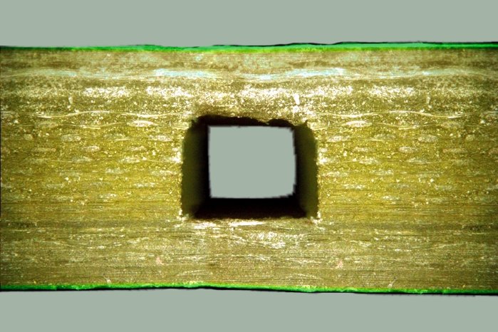
ANDUS ELECTRONIC specialises in integrating a wide variety of technologies into PCBs. Just one example is the company’s PCR reactors (PCR is the abbreviation for Polymerase Chain Reaction). The biochemical sequencing of polymers is a temperature-dependent process: The faster the temperature cycles get, the more efficient the analysis becomes. ANDUS have developed a special PCB for this application that is able to store high quantities of heat over a very short time in a 3 mm (approx. 1/8“) wide copper sheet. Semiconductor-based micro-peltier elements are directly applied to this copper sheet and provide the enormous heat flows required.
A further extremely important topic in medical and/or biochemical applications is copper-free electronics. On one hand, copper is the standard material in PCB manufacturing; on the other hand, it can not be used in systems with biologically active substances as it is cytotoxic. Therefore, ANDUS has developed a process that replaces copper on sensor and actor electrodes by aluminium or stainless steel. As the company has a long-term experience in the area of flexible PCBs, ANDUS is able to realise flexible printed circuits with conductive tracks from stainless-steel.
A further, biocompatible alternative to copper is gold. ANDUS uses this metal for its Microflex adapters for brain research: Two foil straps with a width of 1 mm (approx. 1/24“) are used to contact a total of eight parallel signals. The contacts are gold-plated and only 60 µm wide.
ANDUS also manufactures x-ray ionisation detectors for image-guided medical and industrial analytics in PCB technology. Furthermore, simple capacitive sensor structures can easily be structured on PCBs in most cases. Thus it is possible to combine the sensor and the interpretation electronics on the same PCB. Today, this technology is used for the capacitive measurement of humidity in tissue or when measuring conductivity or electric potentials. However, the technology can also be used in diagnostics and even cosmetics applications.
With a PCB for a micro-light, ANDUS impressively proves that electronic modules do not always need to be big. The double-sided board with several vias is only 50 µm thick. The PCB’s diameter of 0.8 mm (approx. 1/32“) is about the diameter of a drawing pin.
Currently, there is a strong trend towards PCBs that partly assume the thermal management of the module by using thick copper layers, massive copper or aluminium as the head distribution media. As many of these technologies and applications are not yet common knowledge, ANDUS is currently strengthening its training and education efforts.
More information can be found on the internet: http://www.andus.de
<<Company Profile>>
For the past 40 years, ANDUS ELECTRONIC has be focussing on manufacturing prototypes and small series of high-end PCBs in all technologies available. Being able to combine this wide variety of technologies is the company’s core stronghold. Apart from multilayer boards with buried vias and micro-vias, ANDUS has been a supplier of flexible and rigid-flexible PCBs for the past 25 years. Some 10 years ago, the company started to supply impedance-controlled substrates, partly with RF materials. The company is based in Berlin-Kreuzberg.


